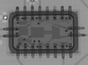
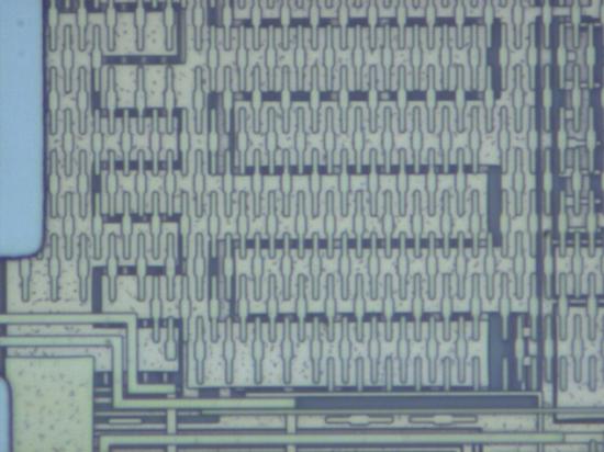
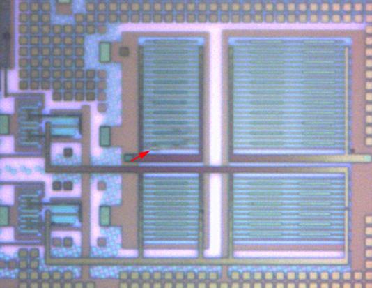
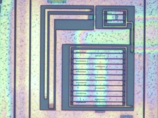
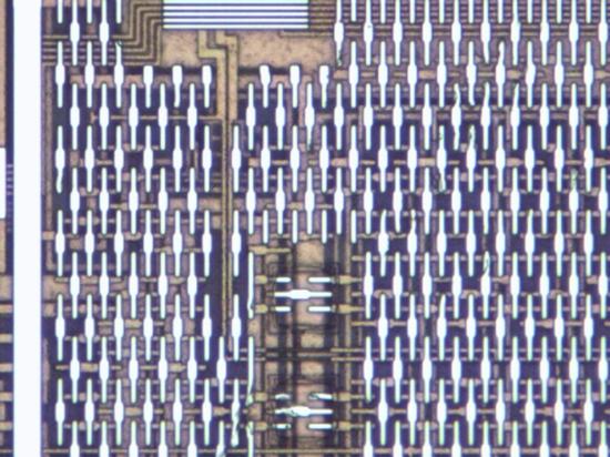
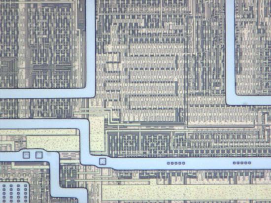
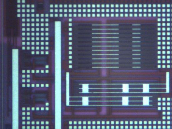
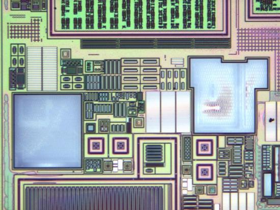
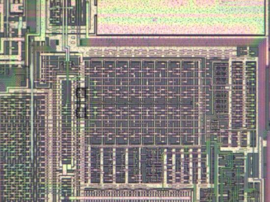
Deprocessing

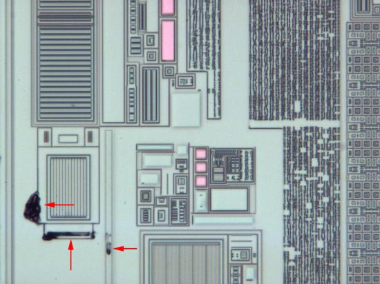
Priority Labs provides a variety of failure analysis techniques for localizing failure sites. Failures can be localized using liquid crystal which will detect any localized heating due to a failure mechanism such as junction damage, gate oxide rupture, reflowed metallization due to over-current events, bridged metal interconnects, polysilicon filaments, electrostatic discharge (ESD) damage, electrical overstress (EOS) damage, and much more. Priority Labs has both back-side and front-side light/photon emission microscopy (LEM/PEM) capability. Our light emission microscope is mounted to a full Micromanipulator probe station within a light proof dark-box on a floating table for versatility and maximum precision and resolution. Using a cooled CCD sensor with 280x1024 resolution, an emission site can be isolated down to a single transistor. Some defects that can be detected with light emission microscopy are as follows:
- Contact spiking
- Hot electron effects
- CMOS latch-up
- Oxide leakage
- Polysilicon filaments
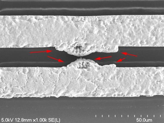
- Silicon mechanical and ESD damage
- Saturated bipolar transistors
- Analog MOSFETS
- Forward biased diodes (PN junctions)
- Silicon filaments (due to process defects) between devices