Scanning Acoustic Microscopy (SAM) is a non-destructive inspection technique used extensively in electronic failure analysis to detect internal structural defects that are not visible using optical methods. By utilizing high-frequency ultrasonic waves, SAM enables engineers to image subsurface features and interfaces within electronic devices and assemblies, making it particularly valuable for identifying delamination, voids, cracking, and other internal anomalies.
SAM is commonly applied to packaged integrated circuits (ICs), printed circuit board assemblies (PCBAs), advanced semiconductor packages, and molded components where internal integrity is critical to reliability and performance. Because the technique does not require material removal, it is often used early in an investigation to guide subsequent analytical steps.
Principles of Scanning Acoustic Microscopy
SAM operates by directing a focused ultrasonic pulse from a transducer into a sample. As the acoustic wave propagates through the material, it interacts with internal features and material boundaries. When the wave encounters a change in acoustic impedance—such as an interface between dissimilar materials, a void, or a crack—part of the sound energy is reflected back toward the transducer.
The system records the time-of-flight of the reflected signal, which is defined as the time between pulse emission and signal return. Knowing the acoustic velocity of the material allows this time delay to be converted into depth information, enabling precise localization of internal features.
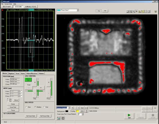
By systematically scanning across the sample surface and recording acoustic responses at each point, SAM generates two-dimensional images that represent internal structures at specific depths. These images can reveal defects that would otherwise remain hidden beneath encapsulation or substrates.
Imaging Modes and Resolution Considerations
SAM systems can operate in several imaging modes depending on the investigation objectives. Common approaches include:
- Reflection (pulse-echo) mode, which detects acoustic reflections from internal interfaces
- Through-transmission mode, which measures sound transmitted through the sample
The resolution of SAM imaging is influenced by transducer frequency, acoustic beam width, and scanning resolution. Higher frequencies provide improved spatial resolution but reduced penetration depth, while lower frequencies allow deeper imaging with lower resolution. Selecting the appropriate frequency involves balancing resolution requirements with material thickness and acoustic attenuation.
Modern SAM systems are capable of imaging features on the order of microns, making them well-suited for advanced electronic packages and fine-pitch interconnect structures.
Common Applications in Electronic Failure Analysis
SAM is widely used to identify internal defects that compromise mechanical or electrical integrity. Typical applications include:
- Detection of delamination between die, mold compound, substrates, and underfill
- Identification of voids within solder joints, adhesives, or encapsulants
- Inspection of cracks caused by thermal cycling or mechanical stress
- Evaluation of package integrity following environmental or reliability testing
- Screening for manufacturing defects prior to destructive analysis
Because many of these defects occur beneath opaque materials, SAM provides critical insight that cannot be obtained through visual inspection alone.
Advantages of SAM in Failure Investigations
One of the primary advantages of SAM is its non-destructive nature. Samples can be inspected without altering their structure, preserving them for additional analytical techniques if required. This is especially important when sample quantities are limited or when multiple investigative steps are anticipated.
SAM also provides rapid feedback, allowing engineers to quickly assess internal integrity and determine whether destructive analysis is warranted. By identifying regions of interest early, SAM helps reduce unnecessary material removal and improves the efficiency of subsequent investigative steps.
Limitations and Practical Considerations
While SAM is a powerful diagnostic tool, it does have limitations. Highly attenuating materials, complex geometries, and surface roughness can affect image quality. Interpretation of SAM images also requires experience, as acoustic contrast may result from geometry, material composition, or both.
For these reasons, SAM is most effective when used in conjunction with other analytical methods. Correlating acoustic findings with design information, construction details, and complementary techniques improves diagnostic confidence and ensures accurate interpretation.
Integrating SAM into a Root Cause Analysis Workflow
In a comprehensive failure analysis workflow, SAM is often used as an early screening and localization tool. Results may be correlated with X-ray imaging, optical inspection, electrical testing, or physical cross-sectioning to confirm suspected defects.
By identifying internal anomalies before destructive analysis begins, SAM helps guide decision-making and ensures that subsequent techniques are applied precisely where they are most effective. This targeted approach supports clear, defensible conclusions and efficient root cause determination.
At Priority Labs, Scanning Acoustic Microscopy is integrated into broader failure analysis and root cause investigations to evaluate internal structural integrity and identify latent defects. When combined with complementary electrical and physical analysis methods, SAM provides valuable insight into failure mechanisms and reliability risks in electronic devices and assemblies.