Dye and Pry
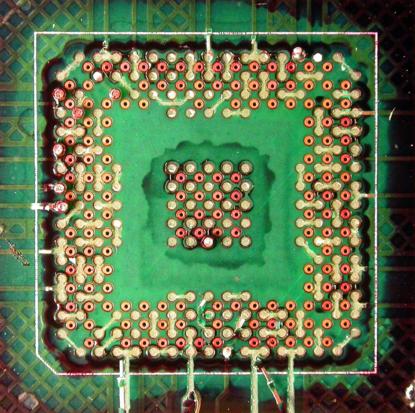
Dye and Pry is a destructive analysis technique used to inspect ball grid array (BGA) and other area-array electronic packages for solder-related defects such as cracking, voiding, and open connections. The method is widely used in printed circuit board (PCB) failure analysis when electrical faults or intermittent behavior are suspected to originate at solder joints that are inaccessible to direct visual inspection.
In a Dye and Pry analysis, a specially formulated penetrant dye is applied to the assembled device. The dye is allowed to infiltrate any cracks, voids, or separations present within the solder joints or interconnect structures. Following dye application, the device is mechanically separated—or “pried”—to expose the solder joints. Areas where the dye has penetrated become visibly stained, clearly revealing the presence and extent of solder defects.
Because BGA solder joints are hidden beneath the package body, conventional optical inspection methods are unable to directly evaluate joint integrity. Dye and Pry provides a direct and unambiguous means of identifying solder cracking, incomplete wetting, voiding, and opens that may contribute to electrical failures. General background on BGA construction and solder joint reliability can be found through IPC, a standards organization for electronics manufacturing.
Priority Labs offers Dye and Pry analysis as part of its comprehensive PCB failure analysis services, supporting investigations into manufacturing defects, field failures, and reliability concerns.
Process Description and Interpretation
The Dye and Pry process begins with careful preparation of the assembled device or PCB. A low-viscosity dye penetrant is applied under controlled conditions to promote capillary action into any existing discontinuities within the solder joints. The dye is selected for its ability to wick into fine cracks and voids without reacting adversely with solder or substrate materials.
After sufficient dwell time, excess dye is removed from external surfaces, and the device is mechanically separated from the PCB. This prying step is performed in a controlled manner to expose the solder joints without introducing new fracture features that could obscure interpretation. Once separated, the solder joints are examined under optical microscopy to identify areas where dye penetration has occurred.
Stained regions within the solder joints indicate pre-existing cracks, voids, or opens that were present prior to separation. The distribution and extent of dye penetration provide insight into the nature of the defect, such as whether cracking is localized or widespread, and whether it initiated at specific interfaces. This information is critical for determining whether solder defects are related to manufacturing processes, thermal cycling, mechanical stress, or material incompatibilities.
Advanced Technical Considerations
From a technical perspective, Dye and Pry analysis relies on the principles of capillary action and fracture mechanics. The ability of the dye to penetrate fine defects depends on crack width, surface energy, and joint geometry. Proper execution requires experience to ensure that dye penetration reflects true defect conditions rather than artifacts introduced during analysis.
Dye and Pry is frequently used in conjunction with other analytical techniques. X-ray inspection may be performed prior to Dye and Pry to identify areas of interest, such as voided joints or suspect interconnects. After prying, optical inspection may be supplemented with scanning electron microscopy (SEM) to further examine fracture surfaces or confirm crack morphology. Additional information on solder joint failure mechanisms and inspection methods can be found through ASM International.
Because Dye and Pry is a destructive technique, careful planning is essential. Priority Labs works with customers to define analysis objectives and determine when Dye and Pry is appropriate within the overall investigation. The technique is particularly effective when electrical opens or intermittent failures are suspected but cannot be conclusively identified through non-destructive methods alone.
Dye and Pry is also useful for evaluating solder joint reliability in response to thermal cycling, vibration, or mechanical loading. Patterns of cracking revealed through dye penetration can help distinguish between fatigue-related failures and defects caused by poor solder wetting, void formation, or assembly process variations. Industry guidance on solder joint reliability and failure modes is available through JEDEC.
Role in Failure Analysis Workflows
At Priority Labs, Dye and Pry is integrated into a structured PCB failure analysis workflow. Results from Dye and Pry are interpreted by experienced analysts who understand the limitations of the technique and how to correlate findings with electrical behavior, manufacturing history, and service conditions. Care is taken to differentiate between true failure mechanisms and secondary damage resulting from mechanical separation.
By clearly revealing solder defects that are otherwise hidden, Dye and Pry provides definitive evidence of interconnect integrity—or lack thereof. This information supports accurate root cause determination and helps guide corrective actions related to assembly processes, materials selection, or design changes.
Through disciplined execution and experienced interpretation, Priority Labs provides Dye and Pry analysis that supports reliable identification of solder joint defects and contributes to clear, defensible engineering conclusions. Dye and Pry remains a valuable tool for exposing hidden interconnect failures in modern electronic assemblies where direct inspection is not possible.
Related Services: