Deprocessing
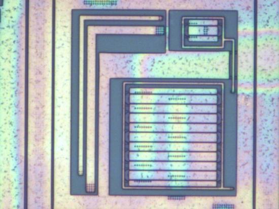
Deprocessing is a controlled material removal technique used in semiconductor failure analysis to expose internal device structures layer by layer. The process enables direct access to metallization layers, dielectric films, vias, contacts, and active device regions for detailed inspection and analysis. At Priority Labs, deprocessing is used to support failure localization, construction analysis, process evaluation, and device characterization for a wide range of integrated circuit (IC) technologies.
Modern semiconductor devices consist of multiple thin-film layers with complex geometries and material stacks. These internal structures are not accessible through external inspection and are often obscured by passivation layers, interconnect stacks, and dielectric films. Deprocessing selectively removes these layers in a controlled manner, allowing analysts to visually examine and document device construction and identify defects or anomalies associated with failure mechanisms.
Deprocessing is frequently applied after an electrical fault has been identified or localized to a general region of interest. By progressively removing material, analysts can observe changes in device structure, identify abnormal features, and correlate physical evidence with electrical behavior. General background on semiconductor device structures and fabrication can be found through the Semiconductor Industry Association (SIA).
Deprocessing Techniques and Methodology
At Priority Labs, deprocessing is performed using a combination of mechanical, chemical, and plasma-based techniques, selected based on device technology, materials, and analytical objectives. Material removal is carried out incrementally to maintain control and minimize the risk of damaging features of interest. Each step is documented to preserve context and support accurate interpretation.
Chemical deprocessing may involve the use of acids, bases, or solvents to selectively remove specific materials such as passivation layers, dielectrics, or metallization. Mechanical polishing or lapping may be used to thin samples or expose specific layers, while plasma etching techniques can provide fine control for removing thin films. The selection and sequencing of these methods are critical to avoid introducing artifacts or obscuring failure evidence. Reference information on thin-film materials and etching processes can be found through ASM International.
As layers are removed, the exposed surfaces are examined using optical microscopy or scanning electron microscopy (SEM). This stepwise inspection allows analysts to track the progression of features through the device stack and identify abnormalities such as voids, opens, shorts, hillocks, or irregular geometries. Deprocessing is especially valuable for evaluating interconnect integrity and identifying defects that originate within buried layers.
Applications in Failure Analysis
Deprocessing is commonly used to investigate a wide range of semiconductor failure mechanisms. These include junction damage, gate oxide rupture, reflowed or displaced metallization resulting from over-current events, bridged metal interconnects, and polysilicon filaments. Many of these defects occur within internal layers and cannot be detected through surface inspection alone.
In cases involving electrostatic discharge (ESD) or electrical overstress (EOS), deprocessing allows analysts to examine damage propagation paths and identify the precise structures affected. For example, melted or ruptured metal lines, damaged contacts, or compromised gate oxides can often be revealed only after removing overlying layers. Industry guidance on ESD and EOS failure mechanisms is available through JEDEC.
Deprocessing is also used for construction and process analysis. By examining layer thicknesses, alignment, and material interfaces, analysts can assess whether devices conform to expected fabrication practices or identify variations that may influence performance or reliability. This information is valuable for both failure investigations and competitive or comparative analyses.
Integration with Localization Techniques
At Priority Labs, deprocessing is often integrated with failure localization techniques such as liquid crystal thermography and light/photon emission microscopy (LEM/PEM). These methods are used to identify regions of interest prior to material removal. Once a failure site has been localized, deprocessing can be targeted to that specific area, improving efficiency and reducing unnecessary material removal.
By combining non-destructive localization with controlled deprocessing, analysts can correlate electrical behavior with physical structures more effectively. This integrated approach improves confidence in root cause determinations and reduces the likelihood of misinterpreting secondary damage. Background information on semiconductor failure localization methods can be found through IEEE technical publications.
Role in Analytical Workflows
Deprocessing is inherently destructive and requires careful planning and experienced execution. At Priority Labs, each deprocessing effort is designed to support the broader analytical objectives of the investigation. Analysts evaluate when deprocessing is appropriate, define stopping points, and ensure that sufficient documentation is captured at each stage.
Results from deprocessing are interpreted in conjunction with electrical test data, imaging results, and other analytical findings. This holistic approach ensures that observed physical features are properly linked to functional behavior and failure mechanisms. Through disciplined methodology and experienced interpretation, deprocessing provides critical insight into how and why semiconductor devices fail.
By enabling controlled access to internal device structures, deprocessing remains an essential tool for semiconductor failure analysis. Priority Labs leverages this technique to support accurate failure localization, detailed construction analysis, and clear, defensible engineering conclusions.
Related Services: