Optical Inspection
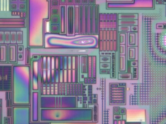
Optical inspection is a foundational analytical technique used to visually examine components, assemblies, and materials for defects, anomalies, and construction details. At Priority Labs, optical inspection is performed across a wide magnification range—from approximately 10× to 2,000×—allowing both low-magnification overview assessment and high-magnification examination of fine features. This capability supports detailed inspection of electronic components, integrated circuits (ICs), printed circuit boards (PCBs), and other engineered materials.
Optical inspection provides direct visual evidence of a sample’s condition and construction. Using high-quality optical microscopes equipped with digital image capture, analysts can document surface features, defects, and dimensional characteristics with clarity and repeatability. Captured images form a permanent record that supports reporting, comparison, and correlation with other analytical techniques. An overview of optical microscopy principles and applications can be found through Olympus Life Science.
At Priority Labs, optical inspection is commonly used as an initial step in failure analysis, quality investigations, and construction analysis. It allows rapid identification of obvious defects such as cracks, contamination, corrosion, misalignment, foreign material, or surface damage. Early identification of these features helps focus subsequent analytical efforts and reduces unnecessary destructive testing.
Inspection Capabilities and Applications
Using advanced optical microscopes, Priority Labs has the capability to inspect advanced integrated circuit technology nodes as well as printed circuit boards of a wide range of sizes and constructions. For ICs, optical inspection can reveal damage to bond pads, metallization layers, passivation coatings, and surface features that may indicate processing issues or failure mechanisms. In PCB assemblies, optical inspection is used to evaluate solder joints, traces, vias, component placement, and surface cleanliness.
Low-magnification inspection is often used to assess overall condition, identify areas of interest, and evaluate large-scale features such as board warpage, discoloration, or mechanical damage. Higher magnifications enable detailed examination of fine features, including microcracks, surface pitting, plating defects, and subtle manufacturing anomalies. The ability to seamlessly transition across magnification levels allows analysts to maintain context while examining localized details.
Digital capture capability is an essential component of optical inspection at Priority Labs. High-resolution images are recorded to document findings, support measurements, and provide visual evidence for reports and presentations. These images are often annotated to highlight defects or features of interest and can be compared against known-good samples or design documentation. General guidance on digital microscopy and image documentation is available from Keyence.
Measurement and Construction Analysis
In addition to visual inspection, Priority Labs maintains in-house measurement capability to support construction analysis, dimensional verification, and competitor benchmarking. Optical measurement tools allow precise quantification of feature dimensions such as trace widths, spacing, pad sizes, coating thicknesses, and defect dimensions. Accurate measurement is essential when evaluating compliance with specifications, identifying process variations, or comparing construction approaches between different products or manufacturers.
Construction analysis using optical inspection is frequently performed to understand how a device or assembly was built, including material selection, layer configuration, and feature geometry. This information is valuable in both failure analysis and competitive evaluation contexts. By combining visual inspection with dimensional measurement, analysts can identify subtle differences in construction that may influence performance, reliability, or cost.
Optical inspection is also used to support and complement other analytical techniques. For example, optical microscopy may be used before cross-sectioning to select optimal section locations, or after decapsulation to examine exposed die surfaces. It is commonly paired with scanning electron microscopy (SEM) for higher-resolution imaging or with electrical testing to correlate visual defects with functional behavior. Background information on the role of optical microscopy in materials and electronics analysis can be found through ASM International.
Role in Analytical Workflows
At Priority Labs, optical inspection is not treated as a standalone activity but as an integral part of a structured analytical workflow. Findings from optical inspection are evaluated by experienced analysts and engineers who understand both the capabilities and limitations of the technique. Care is taken to distinguish meaningful defects from benign features or cosmetic artifacts.
Because optical inspection is non-destructive, it is often used early in an investigation to guide decision-making and prioritize follow-on analyses. This approach improves efficiency, preserves samples, and ensures that more invasive techniques are applied only where they are most informative. When combined with other methods such as X-ray imaging, SEM, or physical cross-sectioning, optical inspection contributes to a comprehensive understanding of device condition and potential failure mechanisms.
Through a combination of broad magnification capability, digital documentation, and precise measurement tools, Priority Labs provides optical inspection services that support reliable failure analysis, quality assessment, and construction evaluation. Optical inspection remains an essential technique for examining the features and details that define the performance and reliability of modern electronic devices and assemblies.