Scanning Electron Microscopy
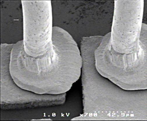
Scanning Electron Microscopy (SEM) is a powerful analytical technique used to examine surface features, microstructures, and defects at high magnification and resolution. Priority Labs currently operates two field-emission scanning electron microscopes (FE-SEM) capable of inspecting and digitally capturing samples at magnifications ranging from approximately 250× to over 100,000×. This capability enables detailed visualization of features that are not resolvable using optical microscopy.
SEM provides high-resolution images by scanning a focused electron beam across the surface of a sample and detecting emitted signals generated by interactions between the electrons and the material. These interactions produce detailed topographical and compositional information that is valuable for failure analysis, defect inspection, materials evaluation, and construction analysis. An overview of SEM fundamentals and operating principles can be found through educational resources such as Thermo Fisher Scientific.
At Priority Labs, SEM is commonly used to examine cross-sections, fracture surfaces, interfaces, coatings, and surface conditions. The technique is particularly effective for identifying features such as cracks, voids, corrosion, contamination, delamination, and morphological anomalies. Because SEM imaging provides significantly greater depth of field than optical methods, it allows complex three-dimensional surface features to be observed with clarity and precision.
SEM analysis is often applied to semiconductors, printed circuit boards (PCBs), electronic components, metals, polymers, and composite materials. It supports both qualitative assessments—such as identifying the presence and morphology of a defect—and quantitative measurements of feature dimensions. This combination makes SEM an essential tool for understanding how materials and structures behave under manufacturing, operational, or environmental stresses.
Advanced Technical Discussion
Field-emission SEM systems use a high-brightness electron source that produces a finely focused beam with excellent stability. Compared to conventional thermionic electron sources, field-emission guns provide improved resolution, especially at low accelerating voltages. This enables high-quality imaging of sensitive or non-conductive samples while minimizing beam damage and charging effects. Additional background on field-emission SEM technology is available from JEOL.
As the electron beam interacts with the sample surface, several types of signals are generated, including secondary electrons and backscattered electrons. Secondary electron imaging is primarily used to reveal surface topography and fine morphological details, while backscattered electron imaging provides contrast based on atomic number differences, making it useful for distinguishing between different materials or phases within a sample.
SEM is frequently paired with energy-dispersive X-ray spectroscopy (EDS) to perform elemental analysis. When the electron beam excites atoms in the sample, characteristic X-rays are emitted that can be detected and analyzed to determine elemental composition. EDS enables localized chemical analysis of defects, inclusions, contaminants, and material interfaces. General information on SEM-EDS analysis is available through Oxford Instruments:
At Priority Labs, SEM is often used following sample preparation techniques such as cross-sectioning, decapsulation, or focused ion beam (FIB) milling. Cross-sectioned samples can be examined to evaluate internal construction features such as layer thickness, interface quality, plating integrity, and defect morphology. Fracture surfaces examined under SEM can provide insight into failure modes, including brittle fracture, ductile overload, fatigue, or environmentally assisted cracking.
SEM is also valuable for surface analysis and materials characterization. It can be used to assess wear patterns, corrosion products, coating adhesion, surface contamination, and processing artifacts. In semiconductor and electronics applications, SEM imaging can reveal damage to metallization, bond pads, interconnects, and passivation layers that may contribute to electrical or mechanical failures.
Digital image capture and documentation are integral to SEM analysis at Priority Labs. High-resolution images are recorded to support reporting, measurements, and correlation with other analytical data. When combined with electrical testing, X-ray inspection, or optical microscopy, SEM results contribute to a comprehensive understanding of device condition and failure mechanisms.
At Priority Labs, SEM is not used in isolation but as part of a structured analytical workflow. Findings from SEM analysis are interpreted by experienced analysts and engineers and integrated with results from complementary techniques. This approach ensures that observations are placed in proper context and that conclusions are based on a complete understanding of the sample and its history.
Through the use of advanced field-emission SEM systems and experienced interpretation, Priority Labs provides detailed surface and materials analysis that supports failure investigations, quality assessments, and root cause determination. SEM remains a critical tool for examining the micro- and nanoscale features that govern performance and reliability in modern materials and electronic devices.