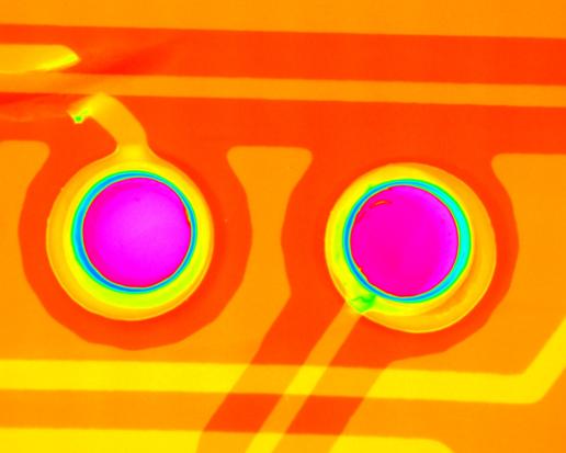
X-ray
Decapsulation is a chemical sample preparation technique used to remove the protective package material from electronic devices in order to expose the internal die and associated structures. At Priority Labs, decapsulation of samples is performed using a variety of acids, bases, and solvents selected based on the specific package materials and investigative objectives. This process enables direct access to the die surface, bond wires, and internal interfaces that are otherwise hidden beneath mold compound or encapsulation materials.
Encapsulation materials—typically epoxy-based mold compounds—are designed to protect devices from moisture, mechanical stress, and environmental exposure. While essential for device reliability, these materials prevent direct inspection of internal features. Chemical decapsulation selectively removes encapsulants while preserving the integrity of the underlying structures, allowing engineers to evaluate device construction, identify defects, and assess potential failure mechanisms. An overview of common semiconductor packaging materials can be found through the Semiconductor Industry Association (SIA).
Decapsulation is widely used in failure analysis, quality investigations, construction analysis, and device authentication. By exposing the die and interconnects, analysts can identify issues such as corrosion, contamination, cracking, metallization damage, bond wire deformation, or manufacturing anomalies that cannot be detected through external inspection alone. When performed correctly, decapsulation provides reliable access to internal features while maintaining the sample in a condition suitable for follow-on analytical techniques.
Advanced Technical Discussion
At Priority Labs, decapsulation is performed using multiple techniques, including manual chemical decapsulation and automated chemical decapsulation using a Nisene Technology JetEtch system. The selection of technique depends on device package type, material composition, geometry, and the level of control required for the investigation. Additional information on automated jet etching systems is available from Nisene.
Manual decapsulation consists of dispensing acid directly onto the surface of a device package to remove the mold compound covering the die. This approach allows precise, localized control of the etching process and is well suited for small sample quantities, non-standard package geometries, or situations where continuous visual monitoring is required. During manual decapsulation, analysts incrementally apply chemical etchants while observing material removal to prevent over-etching or unintended damage to sensitive structures such as bond wires or passivation layers.
After the die has been exposed adequately, the device is rinsed with an appropriate solvent to neutralize and remove residual chemicals. Proper rinsing is critical to stop the etching reaction and prevent chemical residues from affecting subsequent inspection or analysis. The sample is then dried under controlled conditions before further evaluation. Improper rinsing or drying can introduce artifacts that complicate interpretation, making process control an essential aspect of successful decapsulation.
Jet etching is the automated version of chemical decapsulation and uses specialized equipment known as a jet etcher. In this process, a focused stream of heated acid is delivered to the specific area of the package that needs to be removed. The jet etcher provides improved repeatability and consistency by controlling parameters such as temperature, flow rate, and exposure time. Only the target region of the package is exposed to the chemical etchant, while the remainder of the package topside is protected by a chemically resistant rubber gasket. This selective exposure minimizes the risk of unintended damage to adjacent areas.
Chemical selection plays a critical role in both manual and automated decapsulation. Different mold compounds, epoxies, and encapsulants respond differently to acids, bases, and solvents. Reference information on common encapsulation materials and their chemical resistance can be found in materials science literature such as ASM International resources.
In many cases, decapsulation may involve multi-stage processes or combinations of chemicals to achieve optimal results while preserving internal structures. Analysts must account for package thickness, filler content, and internal metallization when defining the decapsulation approach.
Following decapsulation, exposed dies can be examined using optical microscopy, scanning electron microscopy (SEM), or other analytical techniques. Decapsulated samples may also be subjected to additional preparation steps or integrated with results from electrical testing, X-ray imaging, or cross-sectioning. For background on SEM analysis of semiconductor devices, see NIST.
At Priority Labs, decapsulation is performed as part of a structured analytical workflow rather than as an isolated step. Careful planning, controlled chemical exposure, and experienced interpretation ensure that internal features are revealed without introducing artifacts or unnecessary damage. This disciplined approach supports reliable analysis, preserves critical evidence, and enables clear, defensible engineering conclusions.