Electrical Characterization
Electrical characterization encompasses a range of test and measurement techniques used to evaluate the electrical behavior, performance, and integrity of electronic devices and circuits. At Priority Labs, electrical characterization is performed across a wide variety of device types, from discrete components to complex integrated circuits, using both standardized and custom test approaches. These capabilities support failure analysis, fault isolation, and detailed understanding of device behavior under controlled conditions.
Priority Labs performs electrical characterization techniques including curve trace analysis, transistor characterization, and custom bench testing of analog, digital, and mixed-signal devices. These methods are used to identify abnormal electrical behavior, confirm functional failures, and isolate defects that may not be apparent through visual inspection or non-destructive imaging alone. General background on electrical characterization principles can be found through Keysight Technologies, a leading test and measurement company.
Because electrical characterization directly evaluates how a device behaves under bias, it is often the most effective way to determine whether a failure is functional, parametric, or intermittent. This information provides a critical foundation for subsequent physical analysis and root cause determination.
Bench Testing and Device Characterization
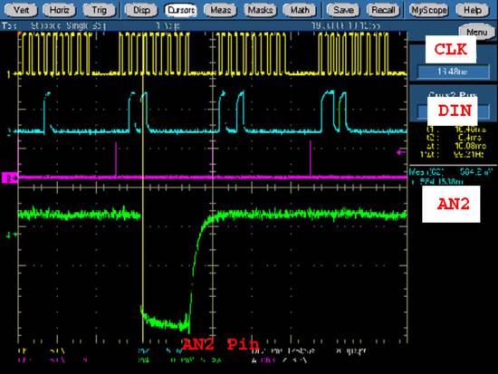
Priority Labs’ analysts and engineers have extensive experience performing bench testing and electrical characterization of analog, digital, and mixed-signal devices. Bench testing may include voltage and current measurements, continuity checks, leakage assessments, timing evaluations, and functional verification under a range of operating conditions. Custom test setups are often developed to replicate field conditions or stress scenarios relevant to the failure under investigation.
Curve trace analysis is frequently used to characterize semiconductor junctions, transistors, and other active devices. By sweeping voltage or current and measuring the resulting electrical response, curve tracing reveals key device parameters and can expose abnormalities such as leakage paths, junction breakdown, or degraded gain. These signatures help differentiate between normal variation and failure-related behavior. An overview of curve tracing techniques is available through Tektronix.
Electrical characterization is also used to compare suspect devices against known-good references. Differences in electrical response can indicate subtle defects, process variations, or damage mechanisms that may not be visible through imaging techniques alone. This comparative approach is especially useful when investigating marginal or intermittent failures.
Fault Isolation and Nodal Analysis
Priority Labs specializes in failure analysis, and as a result places strong emphasis on fault isolation through in-depth electrical analysis. When failures are localized to specific functional blocks or signal paths, nodal analysis is performed to evaluate electrical behavior at internal nodes within a circuit. This level of analysis is essential for identifying the root cause of complex failures in advanced integrated circuits.
To access internal nodes that are not externally available, Priority Labs utilizes Focused Ion Beam (FIB) techniques to perform probe pad deposition and circuit access. Using FIB, conductive material can be selectively deposited to create temporary probe pads or access points on internal interconnects. This capability allows analysts to directly probe signals and voltages within buried circuit structures. Background on FIB-based circuit access can be found through Thermo Fisher Scientific.
Once access points are established, microprobing is performed using an extensive selection of probe stations. These systems support precise placement of probe tips on small geometries and enable controlled electrical biasing during measurement. Priority Labs’ probe stations include cold temperature capability and integrated dark boxes, allowing electrical characterization under reduced noise and controlled environmental conditions.
Advanced Probing Capabilities
Priority Labs is capable of probing small device geometries using probe tips as small as 500 nm, enabling access to fine-pitch features and advanced technology nodes. This capability is essential for analyzing modern semiconductor devices where feature sizes continue to shrink and external test points are limited or unavailable.
Microprobing combined with electrical characterization allows analysts to directly observe signal behavior, voltage levels, and current flow at specific locations within a device. This information can be correlated with schematic data, layout information, and expected device operation to identify discrepancies and isolate faults. In many cases, this approach enables identification of failure mechanisms such as shorted nodes, open interconnects, leakage paths, or damaged transistors.
Electrical characterization may also be performed under varying bias conditions, temperatures, or stimulus patterns to reproduce intermittent or stress-related failures. These controlled variations provide insight into failure sensitivity and help distinguish between permanent damage and condition-dependent behavior. Reference information on semiconductor probing and characterization practices is available through ASM International.
Integration with Failure Analysis Workflows
At Priority Labs, electrical characterization is integrated into a structured failure analysis workflow. It is often one of the first analytical steps performed and may be revisited throughout the investigation as new information becomes available. Electrical findings guide decisions regarding further analysis, such as whether to apply non-destructive imaging, FIB cross-sectioning, or deprocessing.
Results from electrical characterization are interpreted by experienced analysts and engineers who understand both device operation and failure mechanisms. Care is taken to ensure that observed electrical behavior is accurately attributed to physical defects rather than test artifacts or setup limitations.
Through a combination of bench testing, advanced probing, and targeted circuit access, Priority Labs provides electrical characterization services that support reliable fault isolation and root cause determination. Electrical characterization remains a critical tool for understanding device behavior and linking functional failures to underlying physical mechanisms in modern electronic devices.