FIB
Focused Ion Beam (FIB) analysis is a versatile and highly precise technique used in semiconductor failure analysis, device characterization, and design debugging. At Priority Labs, FIB capabilities are provided using an FEI 200 FIB system, enabling device cross-sectioning, ion-induced charge contrast imaging, and device micro-surgery. This platform supports selective milling and deposition of both conductive and insulating materials, allowing controlled modification and inspection of complex device structures.
FIB systems operate by directing a finely focused beam of ions—typically gallium—onto a targeted region of a sample. The interaction between the ion beam and the material allows for localized material removal (milling), deposition, or imaging. Because the beam can be precisely controlled, FIB enables access to internal features at spatial scales that are not achievable using conventional mechanical methods. A general overview of FIB principles and applications is available through Thermo Fisher Scientific, a leading supplier of FIB instrumentation.
At Priority Labs, the FIB system operates across a wide range of ion beam currents—from approximately 1 pA to 20 nA—and supports magnifications from about 1,000× to over 100,000×. This flexibility allows analysts to balance resolution, material removal rate, and beam interaction effects depending on the task at hand.
Cross-Sectioning and Physical Analysis
One of the primary applications of FIB is precision cross-sectioning. Using the ion beam, analysts can create cross-sections through specific regions of interest, ranging from individual transistors to larger features such as die bumps, wire bonds, or interconnect stacks. Unlike traditional mechanical cross-sectioning, FIB cross-sections can be placed with sub-micron accuracy, making it possible to expose very specific device features.
FIB cross-sectioning is commonly used to examine metallization layers, vias, contacts, dielectric interfaces, and failure sites identified through prior localization techniques. The resulting cross-sections can be examined using in situ imaging or transferred for further analysis using scanning electron microscopy (SEM). Reference information on FIB cross-sectioning techniques can be found through JEOL.
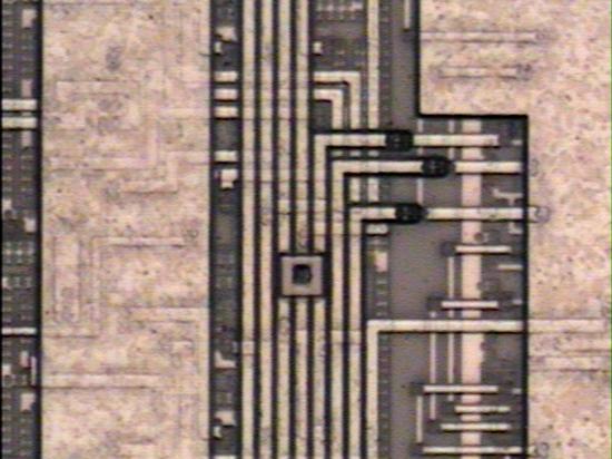
Ion-Induced Charge Contrast (IICC)
Ion-Induced Charge Contrast (IICC) imaging is another powerful capability enabled by FIB analysis. IICC relies on changes in secondary electron emission caused by localized charging effects when the ion beam interacts with semiconductor structures. These contrast variations can be used to determine whether metal traces are electrically connected, shorted, or completely open.
IICC is particularly useful for evaluating interconnect integrity in integrated circuits and identifying subtle electrical discontinuities that may not be visible through conventional imaging. It is often applied during failure analysis to confirm whether suspected cuts, opens, or shorts are present within buried layers. Background on charge contrast imaging techniques is available through ASM International.
Device Micro-Surgery and Circuit Modification
In addition to analysis, FIB enables device micro-surgery, a set of techniques used to physically modify circuits at the micro- and nanoscale. At Priority Labs, micro-surgery applications include circuit isolation through precise cuts, creation of conductive jumpers, selective probe pad deposition, and tap-and-place operations. These modifications allow engineers to isolate signals, reroute connections, or access internal nodes for probing.
Device micro-surgery is frequently used for design debugging and validation. By implementing targeted changes directly on existing devices, engineers can evaluate design hypotheses without committing to costly and time-consuming mask revisions. As a result, FIB-based micro-surgery provides a low-cost, low-cycle-time alternative to full fabrication changes during development and debug phases. Industry discussion of FIB-based circuit editing can be found through IEEE publications.
Integration with Failure Analysis Workflows
At Priority Labs, FIB analysis is integrated into a broader failure analysis and root cause investigation workflow. FIB is often applied after non-destructive localization techniques—such as electrical characterization, liquid crystal thermography, or light/photon emission microscopy (LEM/PEM)—have identified a region of interest. This targeted approach minimizes unnecessary material removal and preserves critical evidence.
Results from FIB analysis are correlated with electrical test data, layout information, and findings from complementary techniques such as SEM or optical inspection. This correlation ensures that physical observations are properly linked to device behavior and failure mechanisms. Because FIB is inherently destructive, careful planning and experienced execution are essential to achieve meaningful results.
Through the use of advanced FIB instrumentation and disciplined analytical workflows, Priority Labs provides precise access to internal device structures and targeted circuit modification capabilities. Focused Ion Beam analysis remains an essential tool for semiconductor failure analysis, design debug, and detailed device characterization, supporting clear, defensible engineering conclusions.